

Current Issue
Instruction-Level GALS Architecture for Low-Power 8051-Compatible Embedded Systems
Rajakumari Alajangi, Research Scholar
Department of Electronics and Communication Engineering,
University College of Engineering, Science & Technology Hyderabad, JNT University, Hyderabad, Telangana, 500 085, India
email: rkvasanth2007@gmail.com
Department of Electronics and Communication Engineering,
Sreenidhi Institute of Science & Technology, Hyderabad - 501 302, Telangana. India.
email: nms2010@ieee.org
Department of Electronics and Communication Engineering,
University College of Engineering, Science & Technology Hyderabad, JNT University, Hyderabad, Telangana, 500 085, India.
email: lalkishorek@gmail.com
---------------------------------------------------------------------------------
Abstract:
This paper discusses the design and implementation of a globally asynchronous, locally synchronous (GALS) 8051 microcontroller with low power consumption and accurate time management for embedded applications. Unlike the traditional 8051 architecture, the proposed design divides the circuit into two local clock domains, thus eliminating the need for a global clock to synchronize the entire circuit and reducing unnecessary clock skew problems and switching requirements. An asynchronous interface technique is implemented in this proposed design to facilitate reliable communication between clock domains, along with incorporating power-aware methodologies, such as selective activation of blocks and clock gating techniques, to make the circuit power efficient. The complete microcontroller circuit, comprising fetch, decode, and execution stages, was designed using Verilog HDL language and synthesized with the help of Genius software from Cadence using GPDK 90 nm technology. A simulation technique was applied to validate the functionality of the design, and its performance was analyzed based on the area, power consumption, and time delays.
Keywords:
GALS, 8051-inspired microcontroller, dual-clock architecture, asynchronous handshake, clock domain crossing, power-aware architecture, Internet of Things applications.
Today's embedded systems and SoC designs require an architecture capable of delivering high performance while at the same time being energy-efficient and reliable under tight hardware constraints [1]. As the complexity of digital systems increases, the conventional technique of employing one global clock to coordinate all blocks loses its effectiveness [2]. Despite the popularity of synchronous designs, which are attributed to their simplicity and predictability, global clock circuitry poses serious design challenges [3]. Such problems include excessive dynamic power consumption owing to clock toggling, clock skew owing to the distance between modules, difficult timing closure, and poor scalability with increasing system complexity. This is especially important in portable devices, Internet-of-Things nodes, smart sensors, and embedded low-power controllers, as energy efficiency and reliable timing play crucial roles in these applications [4].
To solve the above-discussed problems, the Globally Asynchronous Locally Synchronous (GALS) method of designing a circuit has become quite popular in the last few years [5]. The main feature of GALS designs is that the complete design is divided into various locally synchronous blocks, where each block is designed using its own clock signal. Communication between blocks occurs asynchronously using handshaking protocols instead of a global clock. Thus, GALS designs can be considered a mixture of asynchronous and synchronous circuits. GALS designs help retain the advantages of both approaches, as the ease of implementation and verification of synchronous circuits remains intact, along with a reduced reliance on the global clock tree [6].
This is even more important when designing low-power consumption applications. For example, in a typical microcontroller design, different modules do not remain operational for equal time intervals. While some blocks work constantly, others remain idle for most of the time. Driving all such modules using a common clock leads to unnecessary switching activity and power wastage.[7] In contrast, a GALS-based system allows individual modules or groups of modules to function independently according to their activities and timing requirements. This makes it possible to localize clocking, reduce redundant transitions, and create a more power-aware digital architecture. In addition, when multiple domains communicate through asynchronous handshakes, the system gains flexibility in managing the timing differences between modules without depending on a single clock frequency [8].
In this study, a dual-clock GALS 8051-inspired microcontroller was designed and analyzed as a power-aware, embedded digital system. The proposed architecture is based on the fundamental fetch, decode, and execute operations of a microcontroller; however, instead of placing the entire system under a global clock, the design is partitioned into two local clock domains. One clock domain is assigned to the selected time-critical modules, whereas the remaining modules operate in another clock domain. Communication between the two partitions is performed by employing asynchronous transfers and handshakes to allow the reliable transfer of data across clock domains. This design approach maintains functional correctness during implementation while leveraging the benefits of distributed clocks [9].
The microcontroller design was described in Verilog hardware description language and synthesized using Cadence Genus tool with the GPDK 90 nm standard cell library. The design flow entails RTL modeling, functional verification, synthesis, and analysis of crucial implementation metrics such as silicon area requirements, power dissipation, and clocking behavior of the design. This study focuses on analyzing the impact of applying the GALS paradigm on the aforementioned metrics, depending on the operating frequencies of the design [10].
Furthermore, another key aspect of this study concerns the potential applicability of the presented concepts in the contemporary world of IoT-oriented resource-limited systems, where power efficiency is valued higher than the maximum throughput. Microcontrollers employed in various monitoring, sensing, wearable electronics, and smart controller tasks must be designed to function with minimal power while retaining their basic digital performance. Therefore, a GALS-based approach is promising because of its modularity, increased ability to control switching activity, and integration of extra low-power features such as clock gating and domain activation. Consequently, this study not only implements a concept but also evaluates the GALS methodology itself, which can serve as a basis for future research [11].
The primary goal of this study is to prove the effectiveness of utilizing a GALS-based architecture in the development of a multi-clock microcontroller, and thus, reduce the drawbacks typical of conventional global clock solutions. By combining locally synchronized computation, asynchronous communication between different clock domains, and an intention to increase the energy efficiency of the designed microcontroller, this study will prove to be a valid contribution towards achieving the stated aim, which will further be supported by the results obtained via simulation and synthesis-based analysis [12].
With the development of system-on-chips, which have become more complicated and have a high integration density, clock distribution has become challenging. Although conventional synchronous systems have several advantages, such as being deterministic and easier to design verification, they have significant disadvantages, such as clock skew, dynamic power consumption, and scaling difficulties due to shrinking feature sizes [13]. To overcome these challenges, a Globally Asynchronous, Locally Synchronous (GALS) architecture design style that breaks down a large synchronous design into smaller clocked islands and connects them asynchronously was introduced as a solution [14]. The basic concept of using a GALS design architecture as a method for simplifying SOC designs by breaking up clocking domains while maintaining data integrity was proposed by Muttersbach et al. [15].
Based on this, Law et al. [16] showed how modeling and synthesis techniques can be used for asynchronous pipelines, demonstrating the effective implementation of handshaking in VLSI systems. In this study, we propose a synthesis technique that ensures the reliable operation of mixed-timing circuits. Subsequent surveys and overviews have confirmed that GALS architectures offer greater modularity, more flexible timing, and greater scalability than deep-submicron circuits. Collectively, these findings suggest that combining locally synchronous circuits with asynchronous interfaces is a more viable design approach than fully synchronous and asynchronous approaches [17].
Subsequent studies have emphasized the significance of power management in GALS design [18]. Rajakumari et al. [19] outlined methods for minimizing leakage power in GALS through the power gating of modules that are not currently in use. The researchers demonstrated how power gating could benefit from asynchronous wrapper signals, which, apart from serving their intended purpose of data communication, can be used to transition module states and manage power consumption efficiently without jeopardizing timing. Moreover, Rajakumari et al. [20] extended their contribution by proposing four-phase handshaking protocol schemes, plausible clock techniques, and power gating sequences for GALS circuits [21].
On the circuit side, Agarwal et al. [22] provided insights into the different leakage mechanisms in nanoscale CMOS circuits, along with possible approaches for mitigating power consumption in deep-submicron circuitry during the standby mode. All these ideas apply to GALS-based low-power systems, where individual modules can be deactivated to decrease leakage and unnecessary switching. In addition, Goldman et al. [23] released the Synopsys Open Educational Design Kit, which facilitated educational purposes in designing ASICs using the synthesis, placement, and routing flow with standard cells.
Previous studies have shown that GALS system design enables lower power consumption, better timing scalability, and modularity in recent VLSI architectures [24]. Previous research has proven the effectiveness of asynchronous wrappers, handshaking protocols, leakage-aware designs, and power-gating methods for large-scale SoCs and novel designs [25]. However, practical demonstrations integrating these ideas into a compact 8051-inspired microcontroller with dual clock domains, asynchronous communication, and synthesis-based evaluation remain limited [9]. The present study builds upon these studies by implementing a GALS-based microcontroller architecture and analyzing its area, power, and timing behavior using a Cadence Genus-driven design flow in 90 nm technology.
The proposed work focuses on the design and implementation of a dual-clock GALS 8051-inspired microcontroller and its extension to a power-aware IoT controller for low-power embedded applications. The architecture was modelled in Verilog HDL and evaluated using a synthesis-driven design flow in Cadence Genus with the GPDK 90 nm standard-cell library. The methodology combines architectural partitioning, asynchronous inter-domain communication, control-based operation, power-aware activation, and hardware-oriented verification to achieve reliable and energy-efficient system behavior.
A. System Overview
The proposed architecture follows the classical fetch-decode-execute organization of a microcontroller while incorporating the Globally Asynchronous, Locally Synchronous (GALS) principle to reduce the dependency on a single global clock. The system consists of major RTL modules, such as the Program Counter (PC), Program Memory (PMem), Instruction Register (IR), Control Logic, Data Memory (DMem), Data Register (DR), Arithmetic Logic Unit (ALU), accumulator (Acc), and Status Register (SR), all integrated into a structured datapath suitable for synchronous local operation and asynchronous global interaction. In addition to the microcontroller core, the design methodology also extends toward a power-aware control scheme suitable for IoT-oriented staged operation, where modules are activated only when required.
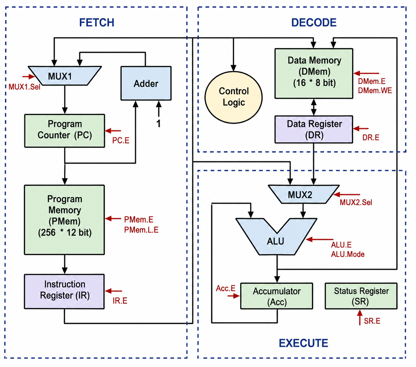
Figure 1. Architecture Design for the Proposed GALS Microcontroller
| Block | Function |
|---|---|
| Program Counter (PC) | Generates the address of the next instruction, and the instruction is fetched from the memory. |
| Program Memory (PMem) | It stores the instruction sequences. |
| Instruction Register (IR) | It holds the fetched instruction for decoding purposes. |
| Control Logic | The instruction is decoded, and control signals are generated. |
| Data Memory (DMem) | Stores intermediate or operand data. |
| ALU | Holds ALU input/output data. |
| Accumulator | Multivariate time-series |
| Async FIFO | Data are transferred safely across clock domains. |
| FSM Controller | The control LOAD, FETCH, DECODE, and EXECUTE sequencing were performed. |
B. Clock-Domain Partitioning
To implement the GALS concept, the microcontroller is divided into two locally synchronous clock domains. The first domain, clk_pmem_alu, is assigned to the Program Memory and ALU-related datapath, whereas the second domain, clk_rest, drives the remaining modules, such as the control logic, data memory, and internal registers. This approach helps simplify the complexity of the global clock tree, confines the timing issues into smaller blocks, and enables the implementation of a low-power modular architecture. The capability of operating each region of functionality at different timing constraints makes the design more scalable and suitable for low-power embedded applications.
| Clock Domain | Major Blocks |
|---|---|
| clk_pmem_alu | Program Memory, ALU-related datapath |
| clk_rest | Control Logic, Registers, Data Memory, FSM |
C. Asynchronous FIFO and Inter-Domain Communication
Because of the presence of two clock domains that work independently, the direct transfer of data is unsafe. To address this problem, an asynchronous FIFO is added between these stages to ensure that the data or instructions are properly transferred from one clock domain to the next. The FIFO acts as a buffer interface. The inclusion of this mechanism for communication between clock domains is crucial to this design methodology, as it allows local synchronous blocks to communicate independently of the global clock signal.
D. FSM-Based OperationThe operation of the system is performed with the help of an FSM, which manages the flow of information in the microcontroller. These states include LOAD, FETCH, DECODE, and EXECUTE. In these processes, the instructions undergo loading into the memory, fetching, decoding in the control unit, and finally, execution by the ALU and other components of the data path. Through the operation using this state mechanism, the operation within the microcontroller is organized properly, providing a well-defined control structure for the validation and synthesis.
E. Power-Aware IoT Controller OperationTo make the architecture scalable for embedded and Internet of Things devices that require less power, the control strategy is based on a power-sensitive-activation scheme. With this design, the controller is kept inactive in the case of a reset or low-power mode and activates various functional blocks once the conditions have been met. After activation, the controller enters a series of stages, including sensing, memory access, processing, and communication with signals denoted as sensor_req, mem_wr_req, mem_rd_req, proc_req, and comm_req, respectively.
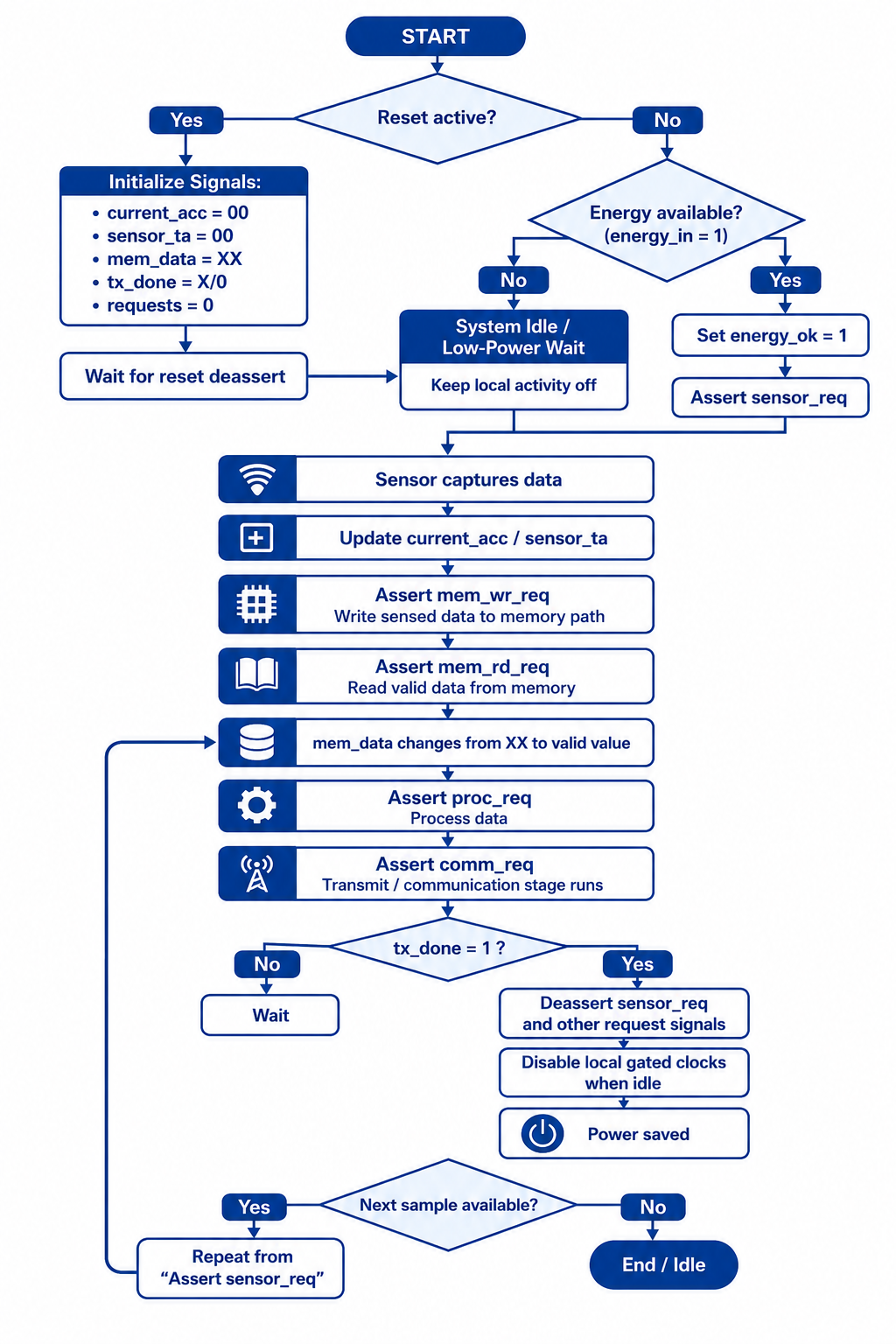
Figure 2. Operational Flowchart of the Power-Aware Controller
Power-aware IoT actions can be further described in the form of a timed sequence starting from reset, detecting energy availability, gradual activation of sensing, memory, processing, and communication blocks, and ending with entering an idle state. Sequencing in stages highlights that the design is not only functional but also well-organized to minimize dynamic switching within inactive regions.
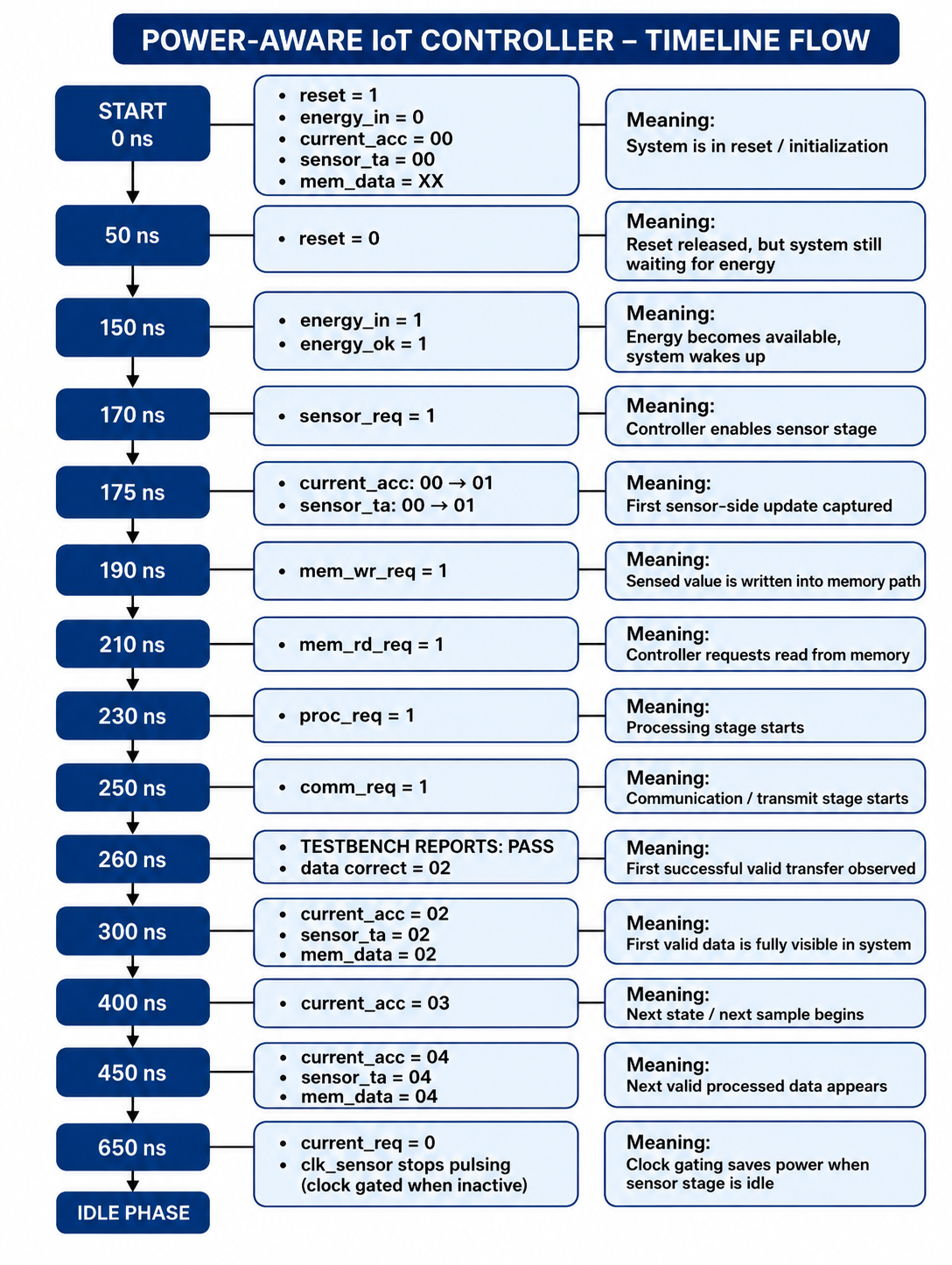
Figure 3. Timeline Flow of the Power-Aware IoT Controller
F. RTL Implementation and VerificationAll functional modules in the proposed design were modeled in Verilog HDL and tested through simulations prior to synthesis. The stimulus used in the testbench consisted of reset signals, initialization, and functional operations to study the changes in signals on the data path, control circuitry, and asynchronous interface. The microcontroller module was tested for correct functionality by simulating the fetch, decode, and execution stages and arithmetic and logic unit functions. In contrast, the power-aware controller was tested for proper block operation and energy-aware functionality.
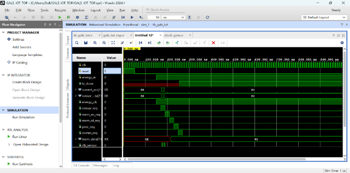
(a) Initial interval showing the reset and start-up behavior.
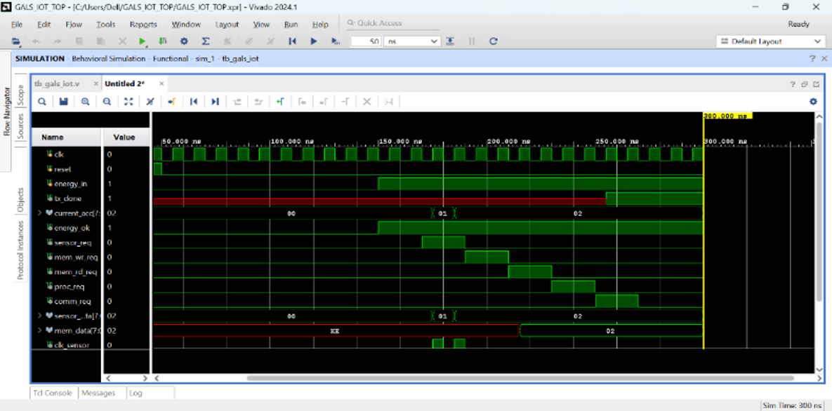
(b) Intermediate interval showing request sequencing and data transfer.
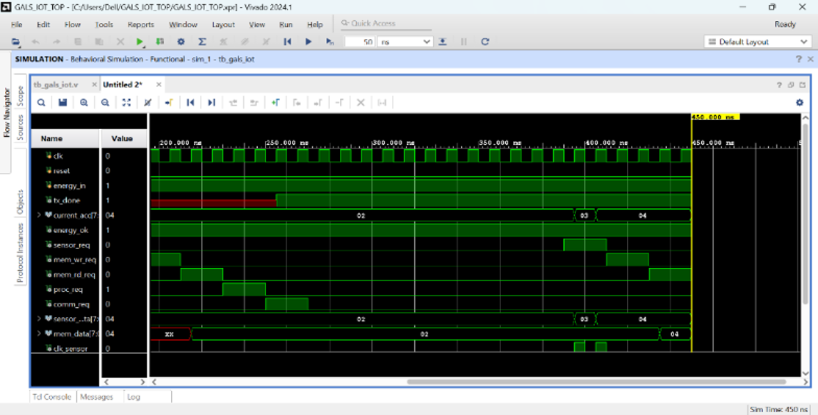
(C) Later interval showing processed output updates and steady operation
Figure 4. Functional Simulation Waveforms of the Proposed Controller
G. Synthesis FlowFollowing functional verification, the RTL was synthesized using Cadence Genus together with the GPDK 90 nm library. The process entails loading the RTL, reading the library, elaboration, application of constraints, optimization, and generation of area, power, and timing reports. The design was evaluated at various frequencies, including 100, 200, and 300 MHz, to analyze its operation under different frequencies and validate whether the proposed design can be implemented practically.
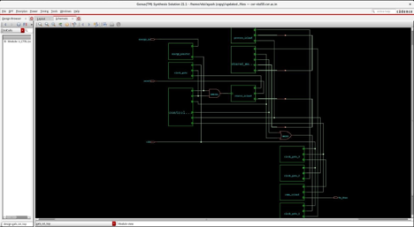
Figure 5. Synthesized Schematic of the Proposed Power-Aware Controller
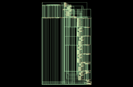
Figure 6. Synthesized Schematic of the Dual-Clock Microcontroller
| Parameter | Conventional Synchronous | Proposed GALS | Improvement |
|---|---|---|---|
| Operating Frequency | 100 MHz | 100 MHz | — |
| Dynamic Power | 12.5 mW | 9.8 mW | 21.6% Reduction |
| Leakage Power | 1.2 mW | 1.3 mW | Slight Increase |
| Total Power | 13.7 mW | 11.1 mW | 18.9% Reduction |
| Area Utilization | 100% | 108% | 8% Overhead |
| Clock Domains | 1 | 2 | Improved Modularity |
| Communication Delay | Low | Moderate | Due to FIFO synchronization |
| Switching Activity | High | Reduced | Lower clock toggling |
The proposed GALS architecture offers lower dynamic power dissipation and switching activity than traditional synchronous designs. Although there is some area overhead due to the extra synchronization circuits, the GALS architecture provides better energy efficiency and scalability than the synchronous design.
H. Evaluation Metrics
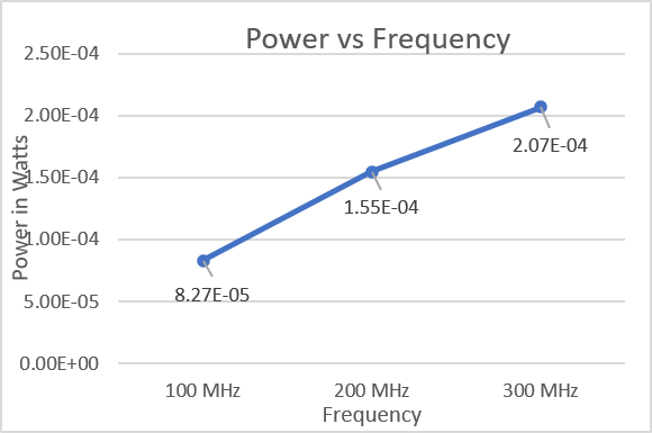
Figure 7. Power Versus Frequency Characteristics
Finally, the proposed solution was evaluated through functional simulations and synthesis metrics, such as area, power, and timing. Functional waveforms ensure proper sequencing and intermodule communication, whereas synthesis reports are used to assess hardware cost and power-performance characteristics at different frequencies. Thus, the proposed methodology was verified in terms of both logical correctness and its physical feasibility.
The proposed GALS-based microcontroller architecture was designed using synthesizable RTL code and evaluated by applying synthesis tools provided by Cadence Genus on a 90 nm GPDK process node. The evaluation included functionality validation and a comparative analysis with a traditional clocked-synchronous microcontroller architecture.
The simulation confirmed the proper functionality of the architecture during instruction fetching, arithmetic operations, memory access, and communication with peripherals. The processor and memory subsystems were operated in separate clock domains with asynchronous FIFO communication to ensure reliable data exchange. The successful coordination of communication via an asynchronous handshake prevents metastability issues.
The analysis revealed a significant improvement in the dynamic power usage of the designed GALS framework compared to that of a conventional synchronous system. This improvement is due to the local clocks and the choice of the functional module activation. Because the new system is not based on global synchronization, it uses only the required functional islands when performing operations; thus, extra switching-off activities are prevented.
The timing analysis results showed the stability of the clock domains in terms of the setup and hold times without any problems arising in the process. Although the addition of asynchronous circuitry created an area overhead in the designs, it was justified because of the improvements in the power efficiency.
This study successfully implements a dual-clock GALS-based microcontroller resembling the classic 8051 microcontroller, which demonstrates proper functionality, timing feasibility, and superiority to a traditional microcontroller in terms of its suitability for low-power digital systems. Splitting the architecture into two domains with their own local clocks and enabling their interaction via asynchronous interfaces decreases the reliance on a unified clock and helps structure the timing behavior. The simulation and synthesis results demonstrate the correctness of the operations at all significant instruction-processing stages and support the claims regarding the practicality of the proposed architecture.
The key result achieved is that using a dual-clock architecture allows obtaining greater efficiency in terms of dynamic power compared to a similar single clock architecture. This increase in efficiency by approximately 20% is demonstrated in the design section. Although extra area cost is incurred owing to the synchronization and asynchronous communication mechanisms, the gain obtained in power efficiency and the possibility of scaling make this architecture more advantageous. Hence, this study demonstrates the success of the architecture implementation and its superiority over traditional architecture.
| Acknowledgments | : | Not applicable. |
| Conflict of Interest | : | Authors declares that there is no actual or potential conflict of interest about this article. |
| Consent to Publish | : | Authors agree to publish the paper in the Ci-STEM Journal of Advanced Materials and Computing. |
| Ethical Approval | : | Not applicable. |
| Funding | : | Authors claims no funding was received. |
| Author Contribution | : | Both the authors confirms their responsibility for the study, conception, design, data collection, and manuscript preparation. |
| Data Availability Statement | : | The data presented in this study are available upon request from the corresponding author. |
REFERENCES:
- D. I. Lazorenko and A. A. Chemeris, “Low-Power Issues for SoC,” Sept. 2006, pp. 1–3. doi: 10.1109/isce.2006.1689463.
- G. Hazari, M. P. Desai, A. Gupta, and S. Chakraborty, “A novel technique towards eliminating the global clock in VLSI circuits,” Ieee Comput Soc, Jan. 2004, pp. 565–570. doi: 10.1109/icvd.2004.1260979.
- E. G. Friedman, “Clock distribution networks in synchronous digital integrated circuits,” Proc. IEEE, vol. 89, no. 5, pp. 665–692, May 2001, doi: 10.1109/5.929649.
- M. Cochet, G. Lallement, F. Abouzeid, and P. Roche, “Clock Generation and Distribution for Low-Power Digital Systems,” Crc, 2018, pp. 1–32. doi: 10.1201/9780429507564-1.
- T. Cheng, “Combining synchronous and asynchronous timing schemes for high-performance systems,” IEEE Des. Test. Comput., vol. 24, no. 5, p. 412, Sept. 2007, doi: 10.1109/mdt.2007.158.
- P. Teehan, M. Greenstreet, and G. Lemieux, “A Survey and Taxonomy of GALS Design Styles,” IEEE Des. Test. Comput., vol. 24, no. 5, pp. 418–428, Sept. 2007, doi: 10.1109/mdt.2007.151.
- H. Chiang, D. Giffin, A. Levy, and P. Levis, “Dynamic Multi-Clock Management for Embedded Systems,” Association for Computing Machinery, Nov. 2018, pp. 347–348. doi: 10.1145/3274783.3275176.
- A. Iyer and D. Marculescu, “Power and performance evaluation of globally asynchronous locally synchronous processors,” SIGARCH Comput. Archit. News, vol. 30, no. 2, pp. 158–168, May 2002, doi: 10.1145/545214.545233.
- K.-L. Chang, T. Lin, W.-G. Ho, K.-S. Chong, B.-H. Gwee, and J. S. Chang, “A dual-core 8051 microcontroller system based on synchronous-logic and asynchronous-logic,” Institute Of Electrical Electronics Engineers, May 2013, pp. 3022–3025. doi: 10.1109/iscas.2013.6572515.
- G. Theodoropoulos, “Modeling an Asynchronous Microprocessor,” SIMULATION, vol. 79, no. 7, pp. 377–409, July 2003, doi: 10.1177/0037549703038884.
- E. Beigne, P. Vivet, Y. Thonnart, J.-F. Christmann, and F. Clermidy, “Asynchronous Circuit Designs for the Internet of Everything: A Methodology for Ultralow-Power Circuits with GALS Architecture,” IEEE Solid-State Circuits Mag., vol. 8, no. 4, pp. 39–47, Jan. 2016, doi: 10.1109/mssc.2016.2573864.
- Z. Yu and B. M. Baas, “High Performance, Energy Efficiency, and Scalability With GALS Chip Multiprocessors,” IEEE Trans. VLSI Syst., vol. 17, no. 1, pp. 66–79, Jan. 2009, doi: 10.1109/tvlsi.2008.2001947.
- P. V. Vishnu, A. R. Priyarenjini, and N. Kotha, “Clock Tree Synthesis Techniques for Optimal Power and Timing Convergence in SoC Partitions,” Institute Of Electrical Electronics Engineers, May 2019, pp. 276–280. doi: 10.1109/rteict46194.2019.9016727
- S. Dasgupta and A. Yakovlev, “Comparative analysis of GALS clocking schemes,” IET Comput. Digit. Tech., vol. 1, no. 2, pp. 59–69, Mar. 2007, doi: 10.1049/iet-cdt:20060159.
- J. Muttersbach, T. Villiger, H. Kaeslin, N. Felber, and W. Fichtner, “Globally-asynchronous locally-synchronous architectures to simplify the design of on-chip systems,” Institute Of Electrical Electronics Engineers, Sept. 1999, pp. 317–321. doi: 10.1109/asic.1999.806526.
- C.-F. Law, B.-H. Gwee, and J. S. Chang, “Modeling and Synthesis of Asynchronous Pipelines,” IEEE Trans. VLSI Syst., vol. 19, no. 4, pp. 682–695, Apr. 2011, doi: 10.1109/tvlsi.2009.2039501.
- C. K. Ong, M. T. Mustaffa, and L. H. Goh, “Asynchronous to synchronous: A design methodology,” Institute Of Electrical Electronics Engineers, Sept. 2011, pp. 255–260. doi: 10.1109/isiea.2011.6108711.
- V. B.V.P, K. Kishore, N. Sharma, and J. Mishra, “A Novel Approach to Minimize Spare Cell Leakage Power Consumption During Physical Design Implementation,” Zenodo (CERN European Organization for Nuclear Research), Dec. 2011, doi: 10.5281/zenodo.5801027.
- Alajangi Rajakumari, N. Murthy Sharma, and K. Lal Kishore, “A Novel Approach to Reduce Leakage Power in GALS System architectures,” International Journal of Computer Applications, vol. 36, no. 5. pp. 12–18, Dec. 2011.
- A. Rajakumari, N. S. Murthy Sharma, K. Lal Kishore, and V. K. Petta, “Synthesizing 4-phase handshaking protocol based power gating sequence logic for GALS architectures,” Dec. 2013, pp. 345–348. doi: 10.1109/icspcom.2013.6719810.
- B. V. P. Vasantha Kumar, “A Novel Approach to Minimize Spare Cell Leakage Power Consumption During Physical Design Implementation,” VLSICS, vol. 2, no. 4, pp. 69–80, Dec. 2011, doi: 10.5121/vlsic.2011.2407.
- A. Agarwal, S. Mukhopadhyay, A. Raychowdhury, K. Roy, and C. H. Kim, “Leakage Power Analysis and Reduction for Nanoscale Circuits,” IEEE Micro, vol. 26, no. 2, pp. 68–80, Jan. 2006, doi: 10.1109/mm.2006.39.
- R. Goldman et al., “Synopsys’ open educational design kit: Capabilities, deployment and future,” Institute Of Electrical Electronics Engineers, July 2009, pp. 20–24. doi: 10.1109/mse.2009.5270840.
- M. Krstic, E. Grass, F. K. Gürkaynak, and P. Vivet, “Globally Asynchronous, Locally Synchronous Circuits: Overview and Outlook,” IEEE Des. Test. Comput., vol. 24, no. 5, pp. 430–441, Sept. 2007, doi: 10.1109/mdt.2007.164.
- Y. Thonnart, X.-T. Tran, P. Vivet, E. Beigne, F. Clermidy, and J. Durupt, “An asynchronous low-power innovative network-On-chip including design-for-test capabilities,” Institute Of Electrical Electronics Engineers, Oct. 2009, pp. 59–62. doi: 10.1109/atc.2009.5349340.
Authors

Ms. Alajangi Rajakumari received the B.Tech. degree in Electronics and Communication Engineering from Nagarjuna University, Vijayawada, India, in 1997, and the M.Tech. degree in Electronics and Communication Engineering from Jawaharlal Nehru Technological University (JNTU), Hyderabad, India, in 2001. She began her academic career as an Assistant Professor with the Department of Electronics and Communication Engineering, Shadan Engineering College, Hyderabad. She subsequently served in various engineering institutions, contributing extensively to teaching, curriculum development, laboratory instruction, and student mentoring. She has more than 13 years of teaching experience in undergraduate engineering education. Her research interests include Very Large Scale Integration (VLSI) design, with particular emphasis on low-power VLSI architectures, digital integrated circuit design, digital system design, FPGA-based system implementation, CMOS circuit optimization, and embedded system design. Her current research focuses on the development of energy-efficient and high-performance digital hardware architectures for next-generation electronic systems. Ms. Rajakumari has authored and co-authored four research publications, including three papers published in IEEE international conference proceedings and one paper published in a peer-reviewed international journal. Her research contributions are primarily focused on advancing low-power digital design methodologies and VLSI system architectures.

Dr. N.S. Murthy Sharma is a distinguished academician and researcher currently serving as a Professor in the Department of Electronics and Communication Engineering (ECE) at Sreenidhi Institute of Science and Technology, Hyderabad, India. He has over 30 years of academic, research, and industrial experience in the fields of Electronics and Communication Engineering, Microwave Engineering, and Electromagnetics. Dr. Sharma obtained a Model Diploma for Technicians with a specialization in Production of Radio Apparatus from the State Board of Technical Education, Hyderabad, in 1984. He received the B.Tech. degree in Electronics and Communication Engineering from Jawaharlal Nehru Technological University (JNTU) in 1990. He subsequently earned the M.E. degree in Microwave and Radar Engineering and the Ph.D. degree from Osmania University, Hyderabad. He was awarded the Ph.D. degree in 2002 for his significant contributions to the electromagnetic modeling of antennas. From 1996 to 2001, he served as a Scientist in the Research and Technology (R&T) Unit for Navigational Electronics, where he was actively involved in advanced research and development activities. He later joined academia as an Associate Professor and served in that capacity until 2008, after which he was promoted to the position of Professor in the Department of Electronics and Communication Engineering. Dr. Sharma has authored and co-authored numerous research papers published in reputed international journals and conference proceedings, including publications indexed in IEEE Xplore and Progress in Electromagnetics Research (PIER). He has also contributed several technical reports in the areas of electronics and communication engineering. His research interests include electromagnetic modeling, antenna design, microwave and radar engineering, ionospheric studies, wireless communications, and other emerging areas of communication engineering.
Dr. K. Lal Kishore is a distinguished academician and former Vice-Chancellor of Jawaharlal Nehru Technological University Anantapur (JNTUA), India, with over 46 years of experience in teaching, research, and academic administration. He obtained his M.E. and Ph.D. from the Indian Institute of Science (IISc), Bengaluru, and served JNTUH in several key positions, including Professor, Rector, Registrar, Principal, and Head of Department. He has published 228+ research papers, supervised 34 Ph.D. scholars, and authored six textbooks in electronics and VLSI. His research interests include electronic devices, VLSI design, electronic circuits, and instrumentation. He has received numerous prestigious national and international awards, including the Lifetime Achievement Award, Best Teacher Award, and Sir M. Visvesvaraya Award. He is a Senior Member of IEEE, Fellow of IETE, and Fellow of the Institution of Engineers (India), LMISTE, LMISHM and continues to contribute actively to engineering education and research.